


 |
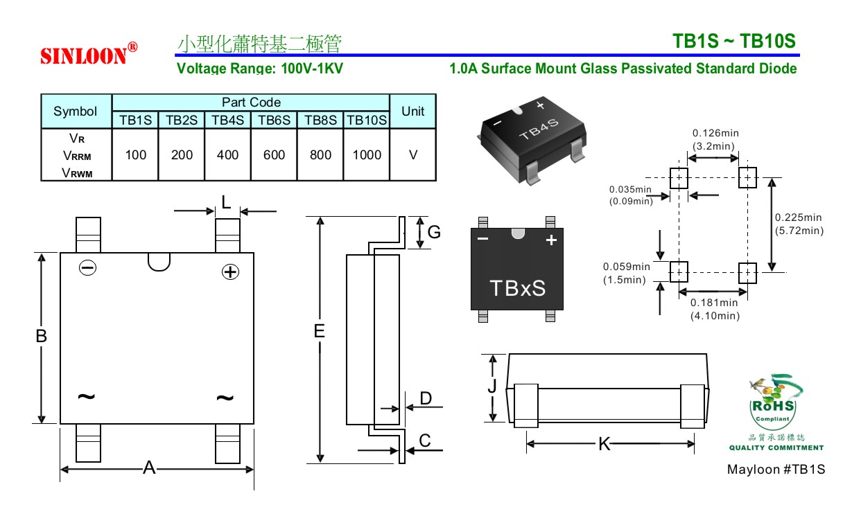
小型化蕭特基二極管 | TB1S ~ TB10S | ||||||||||||||||||
| Voltage Range: 100V-1KV | 1.0A Surface Mount Glass Passivated Bridge Rectifier | |||||||||||||||||||
  TB1S - TB10S 100V-1000V 1.0A TB1S - TB10S 100V-1000V 1.0A |
||||||||||||||||||||
| FEATURE: | MECHANICAL CHARACTERISTICS: | |||||||||||||||||||
| High reliability | Case: TB-S Molded Plastic | |||||||||||||||||||
| Low forward voltage drop | Weight: 0.10 Grams (approx) | |||||||||||||||||||
| High surge current capability | Marking: Type number | |||||||||||||||||||
| Glass passivated die construction | Polarity: As marked on case | |||||||||||||||||||
| Ultra-slim 1.5mm max. case height | Terminals: Plated leads solder able per | |||||||||||||||||||
| Designed for surface mount application | MIL-STD-202, Method 208. | |||||||||||||||||||
| Plastic Material - UL Recognition Flammability | Lead Free for Rohm / Lead free version | |||||||||||||||||||
| Classification 94V-0 | and "LF" suffix to part number. | |||||||||||||||||||
|
SINLOON | |||||||||||||||||||
| Sigle, phase half wave 60Hz resistive or inductive load, for capacitive load, derate current by 20%. | ||||||||||||||||||||
| Parameter at Tamb = 25℃ | Symbol | Part Code | Unit | |||||||||||||||||
| TB1S | TB2S | TB4S | TB6S | TB8S | TB10S | |||||||||||||||
| DC Blocking Voltage: | VR | 100 | 200 | 400 | 600 | 800 | 1000 | V | ||||||||||||
| Peak Repetitive Reverse Voltage | VRRM | |||||||||||||||||||
| Working Peak Reverse Voltage | VRWM | |||||||||||||||||||
| RMS Reverse Voltage | VR(RMS) | 70 | 140 | 280 | 420 | 560 | 700 | V | ||||||||||||
| Average Rectified Output Current @TA=25℃ (1) | Io | 1.0 | 1.0 | 1.0 | 1.0 | 1.0 | 1.0 | A | ||||||||||||
| Non-Repetitive Peak Forward Surge Current 8.3ms Single | IFSM | 30 | 30 | 30 | 30 | 30 | 30 | A | ||||||||||||
| half sine-wave superimposed on rated load (JEDC Method) | ||||||||||||||||||||
| Forward Voltage Diode | @IF = 0.4A | VFM | 0.95 | 0.95 | 0.95 | 0.95 | 0.95 | 0.95 | V | |||||||||||
| @IF = 1.0A | 1.10 | 1.10 | 1.10 | 1.10 | 1.10 | 1.10 | ||||||||||||||
| Peak Reverse Current @TA = 25℃ | IRM | 5.0 | 5.0 | 5.0 | 5.0 | 5.0 | 5.0 | μA | ||||||||||||
| At Rated DC Blocking Voltage @TA = 125℃ | 500 | 500 | 500 | 500 | 500 | 500 | ||||||||||||||
| Typical Junction Capacitance per leg (2) | Cj | 10.0 | 10.0 | 10.0 | 10.0 | 10.0 | 10.0 | pF | ||||||||||||
| Thermal resistance junction to ambient (1) | RθJA | 62.5 | 62.5 | 62.5 | 62.5 | 62.5 | 62.5 | ℃/W | ||||||||||||
| Thermal resistance junction to lead (3) | 25 | 25 | 25 | 25 | 25 | 25 | ||||||||||||||
| Operating and Storage Temperature Range | TJ,TSTG. | -50 to +150 | ℃ | |||||||||||||||||
| Note1 : | Mounted on aluminum substrate PCB with 1.3x1.3mm pad areas. | 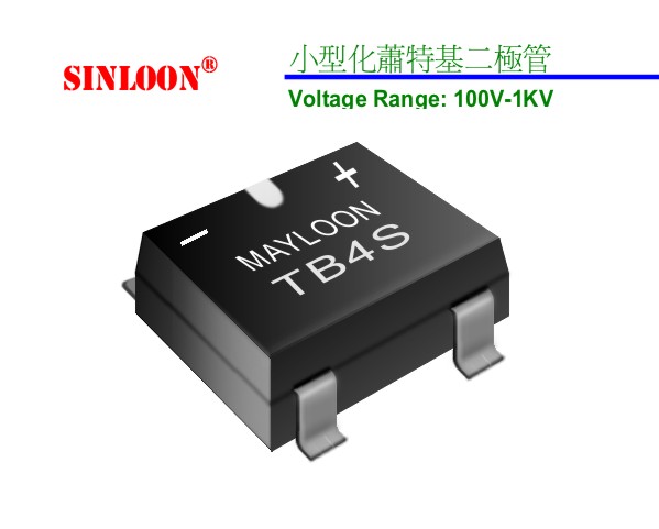 |
 |
|||||||||||||||||
| Note2: | Measure at 1.0 MHz and applied reverse voltage of 4.0V DC | |||||||||||||||||||
| Note3: | Mounted on glass epoxy PCB with 1.3x1.3mm pad areas. | |||||||||||||||||||
Diode
| < 前一個 | 下一個 > |
|---|


